先進封裝Chiplet 技術介紹(視頻)
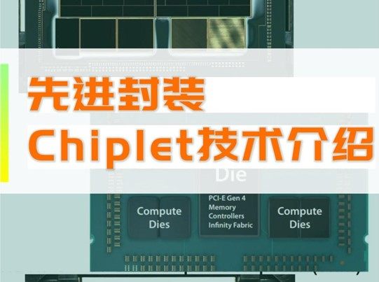
Hello everyone, welcome to semi content. I got a request to talk about chimney, so today's topic is chimney. Let's talk about it. Chimney is a semiconductor technology to use multiple small dyes to achieve target function, which is supposed to be done by one dice dye. Its goal is to reduce product development time and cost by integrating multiple smaller dyes in a package. A chimney is not a package type and it is part of a packaging architecture. With chimney, dice could be integrated into an existing package type, such as 2.5 d, 3 d, fan out, multi chain modules.
大家好,歡迎來到半導體內容。我接到一個講講關于Chiplet的請求,所以今天的話題是Chiplet。我們來談談吧。Chiplet是一種半導體技術,使用多種小芯粒來實現目標功能,將原本應該由一個芯粒來完成的任務,分為多種較小的芯粒集成在一起來實現。從而,減少產品開發時間和成本。Chiplet不是指封裝類型,它是封裝架構的一部分。通過chiplet,多種芯粒可以集成到現有的封裝類型中,例如2.5D、3D、扇出及多芯片模塊。

微信識別二維碼觀看視頻
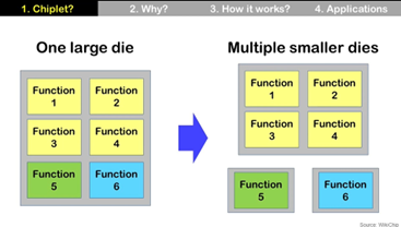
Imagine we have one large die and it has CPU, GPU and other functional blocks all in one die as soc system chip. But it is very expensive and there are many challenges to make these clients die. Fortunately, we can have all these functions by multiple smaller dyes. And economically it is more reasonable. But we need to add interface block to each die, so total die area will be more than one dodge die. That is a brief concept of chimney. So chimney is a good solution for large expensive dye, which is typically for high performance computing, rather than for a small die in smartphone. A silicone note of semiconductor advanced like 45nm,16nm and even 7nm.
想象一下,我們有一個大芯片,它有CPU,GPU,RAM及其它功能塊都在一個芯片中作為SOC系統芯片。但這是非常昂貴的,并且有許多挑戰使這些產品很難量產。幸運的是,我們可以通過多種較小的芯粒來實現所有這些功能,而且這樣在成本上更合理。但是由于我們需要在每個芯粒上添加接口模塊,所以總的所有芯粒總面積將超過全部集成在一個芯片上。這是chiplet的一個簡單概念。因此,Chiplet是大型系統集成芯片的良好解決方案,通常用于高性能計算,而不是智能手機中的小芯片。一種使用先進的半導體制程如45nm、16nm甚至7nm。
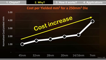
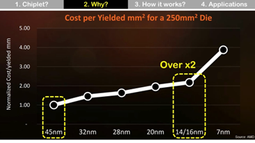
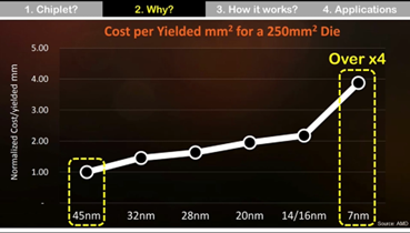
Cost for large dice continues to increase. Cost for a 16mm dye with 250mm2 size is more than 2 times expensive than 45nm die with same die size. And 7nm die is more than 4 times expensive than 45nm die. Now we're talking about 5nm and even 3nm. Then cost revenue increased continuously. That means fabricating large soc dies with advanced silicone node is losing its economical benefit. That is why the industry has started to use chimney again.
隨著大芯粒的成本繼續增加。針對一個250mm2尺寸的芯粒,14或16納米制程的成本是相同尺寸的45納米芯片的2倍以上。而7納米芯片比45納米芯片貴4倍以上。而到我們最近談論的5納米甚至3納米,成本更將不斷增加。這意味著使用先進制程制造大型SoC芯片正在失去其經濟效益。這就是為什么這個行業又開始使用chiplet了。
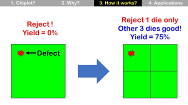
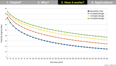
Chimney is to break down a large expensive single die into multiple smaller dyes. How it works? This is simple comparison between one dies die and 4 small dies. If there is a defect at the upper left of the die, then it is risen. One die liseth out of one die. So eld is 0. If we have 4 small dies and there is same defect at the exact same location. Then only one die is risen out of 4 dice and eld is 75%. That means we still can save 30 dice. It is more obvious for belly lies die. It also works for a dialogue at the vapor edge. At the left we have dialogues at the wafer ads for large diet. At the right we also have a dye loss, but smaller dye has higher yield than last dye. This is dialed comparison between one die versus chimney with 2,3 and 4 dies. For a 360mm2 one die we'll have 15% ill but a full chimney design each 99 k millimeters will have 37 yield more than doubles. Even though the total die area of 4 chimney design is more than 10 than one die, the significant yield improvement of chimney is good enough to justify a chimney solution.
Chiplet是將大型的單一芯粒分解成多個較小的芯粒。它是如何工作的?這是一個大芯粒和4個小芯粒之間的簡單比較。如果在芯粒的左上角有缺陷,則整個芯粒就無法使用,所以良率是0。如果我們有4個小芯粒,并且在完全相同的位置存在相同的缺陷。然后4個芯粒只有一個不能使用,良率為75%。這意味著我們仍然可以節省3個芯粒。它也適用于邊緣DIE。在左邊,我們有大量無法使用的邊緣DIE。在右邊,我們也有相類似的損失,但較小的芯粒比較大的芯粒具有更高的良率。這是一個芯粒與chiplet 的有2,3或4個芯粒之間的比較。對于360mm2的一個芯粒,我們僅有15%的良率。但針對4個芯粒的chiplet 設計,良率將是前者的一倍以上。即使4個芯粒的chiplet 設計的總面積比一個大芯粒多出10%,Chiplet的設計明顯提高了良率和合理性。
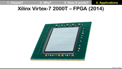
Back in 2014 fpga company gidings made vertex 72000 t and it used 4 smaller chimney dyes rather than one. Dodge fpga. This is AMD epic second generation package and it is a CPU for server using 7nm silicone note technology. Its package size is 58.5mm by 75 point 4mm. Yes, it is big. There are 8 CPUs using 7nm silicon technology and one iodi using 14nm silicon technology at the center. This is Intel xe hpc and it is a GPU using 7nm silicon technology for a supercomputer. Now Intel is using this only in the lab. It has 47 components and include 2 base tiles using Intel's 10nm sofa pin technology. 16 computer tiles using t s m c. Seven nanometer technology.
早在2014年,賽靈思生產的72000,它使用了4個較小的芯粒,而不是1個大芯片。這是AMD史詩級般的第二代封裝,它是使用7nm的服務器CPU。其封裝尺寸為58.5mm乘75.4mm,它非常大。中心有8個使用7nm技術的CPU和一個I/O 芯片使用14nm技術。這是英特爾XE HPC,它里面的GPU使用7nm技術,現在英特爾只在實驗室中使用它。它有47個組件,包括2個基礎芯片使用英特爾10nm技術。16個計算核心使用TSMC的7納米技術。
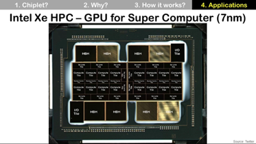
A lambo cache tile using intel's ten nanometer enhanced super pin process. 11 MIB links made by Intel. 2 x link Io tile made by a foundry. 8 HBM memory stacks produced by a dealer manufacturer. It ought to be impossible to build a single chip with these 47 components. Even though chimney has lots of benefit, it also has some challenges. We need to think about die to die interconnection, code design by chip designer and package designer. Easily required tests for small dies will be different from one large dies, etc. Thanks for watching and have a nice day. Bye bye.
11個緩沖使用英特爾十納米技術,2 個I/O芯粒由代工廠代工。8個HBM存儲器堆棧由存儲廠加工。沒有chiplet技術,是不可能將47個芯粒的功能一次性在單個芯片上加工完成的。盡管chiplet有很多好處,但它也有一些挑戰。我們需要思考芯片到芯片的互連,芯片設計師和封裝設計師的協同,多個小芯粒的測試也將非常不同于一個大芯粒的測試等。

微信識別二維碼觀看視頻


